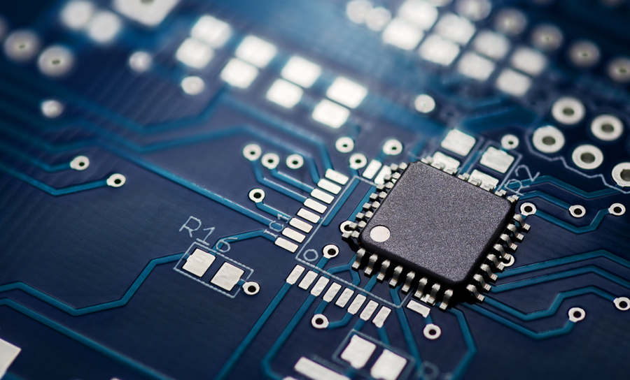
While printed circuit board (PCB) design and PCB fabrication are routinely outsourced, knowing the manufacturing process may help select a manufacturer. Even though PCB manufacturing is a continually evolving process, it is usually based on a set of core techniques such as machining, imaging, plating, etching, and laminating. Apart from its inherent advantages and disadvantages, each of these strategies performs various duties.
Design
Printed circuit board assemblies are often inexpensive, especially in large quantities. Contrary to popular belief, the most expensive and challenging component of the PCB is not its production but rather its design. The PCB assembly design process is a labyrinth of variables, and various factors affect its output. Components must be adequately mapped, copper to board ratios must be constant to minimize waste and warping, distances between tracks and components must be kept consistent to avoid cross-talk or coupling, and track widths must be consistent with signal frequency and current, among other criteria. In other words, printed circuit board engineering is a highly specialized field of work, and circuit board design is frequently the most costly aspect of printed circuit board manufacture. When it comes to board designs that use RF (radio frequency) components, placement becomes critical since the performance of RF assemblies can be considerably degraded if the components are not correctly positioned about the wavelengths of the signals being conveyed.
Machining
The capacity to drill microscopic holes with dimensions measured in hundredths and thousandths of an inch correctly and in huge quantities is crucial throughout the machining phases of printed circuit board manufacture. Numerous boards could not be stacked in the past due to the risk of breaking or distorting the hole walls; however, modern technology allows for simultaneous drilling of several stacked boards without causing damage to the hole walls. Drill bits with a diameter of fewer than 0.0135 inches are often more expensive and less resistant to activewear. Additionally, when the ratio of board thickness to hole diameter increases, plating reliability may suffer. Mechanical or laser drilling is frequently used to create holes, and thinner boards are typically easier to drill to tight tolerances than larger ones. The ease with which laser cut circuit boards may be precisely sliced is gaining popularity, particularly for smaller and more delicate PCBs.
Imaging
Being one of the early circuit board imaging methods, screen printing has remained popular due to its cheap material requirements, low initial capital investment costs, and ability to generate vast quantities of circuit boards in a short period. Nonetheless, its use decreases when working with smaller space and line dimensions, necessitating the employment of particular screens when dealing with narrower line widths and tighter spacing limits, as seen in the following example. Photoimaging is the most popular technique for multilayer and fine-line circuitry applications. It encompasses a range of technologies for producing films, including liquid roller coating, dip or spin coating, hot roll lamination, and electrophoresis. The process of registering circuit images onto a board is highly accurate. The imaging process in PCB assembly is more efficient by using the same tooling equipment for image registration and hole-to-pin alignment. Regardless of its apparent benefits, photoimaging errors can arise for a variety of causes, including the following:
Unintentional movement within a device panel or between separate panels can be caused by stress relaxation in an inner layer.
After repeated use, a tooling system becomes worn, referred to as tool wear. Worn tooling can result in bigger pinholes, resulting in loose components and jeopardizing the circuit board’s integrity.
Increased temperatures and thermal cycling can increase the possibility of etched features protruding from their assigned locations on the board during delamination cycles.
- Proper inner-layer preparation is crucial because excessive pressure applied during the mechanical scrubbing process might stretch or distend the laminate, which is undesirable.
Polyester imaging films may expand or contract in response to exposure to high temperatures and humidity, depending on the temperature and humidity levels in the manufacturing environment.
Some activities may be taken to mitigate the risk posed by these circumstances. Micromodification, which enlarges certain areas of the film to enhance imaging registration, and film stretching, which enlarges printed pictures to compensate for future shrinkage, are two frequently used ways for preserving print accuracy. Micromodification enlarges some areas of the film to aid with image registration. Additionally, operating in a cleanroom atmosphere can help minimize the possibility of pollutants interfering with the scanner’s picture quality.
ChinaPCBOne Technology LTD. is the author of this article on PCB assembly. Find more information, about PCB fabrication.


